- 您现在的位置:买卖IC网 > Sheet目录357 > SP7600EN2-L (Exar Corporation)IC LED DRVR PWM STP-DWN 8HNSOIC
�� �
�
�S� P� 7� 6� 0� 0�
�2� A� 2� 9� V� N� o� n� -� S� y� n� c� .� B� u� c� k� H� i� g� h� P� o� w� e� r� L� E� D� D� r� i� v� e� r�
�ABSOLUTE� MAXIMUM� RATINGS�
�These� are� stress� ratings� only� and� functional� operation� of�
�the� device� at� these� ratings� or� any� other� above� those�
�indicated� in� the� operation� sections� of� the� specifications�
�below� is� not� implied.� Exposure� to� absolute� maximum�
�OPERATING� RATINGS�
�Input� Voltage� Range� V� IN� ................................4.5V� to� 29V�
�Junction� Temperature� Range� ....................-40°C� to� 125°C�
�Thermal� Resistance� θ� JA� ......................................� 59°C/W�
�rating� conditions� for� extended� periods� of� time� may� affect�
�reliability.�
�Input� Voltage� .............................................� -0.3V� to� 30V�
�Lx................................................................-2V� to� 30V�
�FB� .....................................................-0.3V� to� V� IN� +0.3V�
�Storage� Temperature� ..............................� -65°C� to� 150°C�
�Power� Dissipation� (Note� 1)� ...................� Internally� Limited�
�Lead� Temperature� (Soldering,� 10� sec)� ...................� 300°C�
�ESD� Rating� (Lx,� ISET)� ....................................1KV� -� HBM�
�ESD� Rating� (All� other� pins)� .............................2KV� -� HBM�
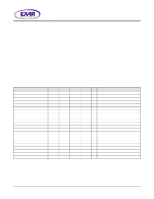
�ELECTRICAL� SPECIFICATIONS�
�Specifications� with� standard� type� are� for� an� Operating� Junction� Temperature� of� T� J� =� 25°C� only;� limits� applying� over� the� full�
�Operating� Junction� Temperature� range� are� denoted� by� a� “?”.� Minimum� and� Maximum� limits� are� guaranteed� through� test,�
�design,� or� statistical� correlation.� Typical� values� represent� the� most� likely� parametric� norm� at� T� J� =� 25°C,� and� are� provided� for�
�reference� purposes� only.� Unless� otherwise� indicated,� V� IN� =� 4.5V� to� 29V,� C� IN� =� 1μF,� T� J� =� –40°C� to� 125°C.�
�Parameter�
�UVLO� Turn-On� Threshold�
�UVLO� Turn-Off� Threshold�
�Min.�
�4.0�
�3.8�
�Typ.�
�4.2�
�4.0�
�Max.�
�4.5�
�4.3�
�Units�
�V�
�V�
�Conditions�
�0°C� ≤� T� J� ≤� 125°C�
�0°C� ≤� T� J� ≤� 125°C�
�UVLO� Hysteresis�
�0.2�
�V�
�Operating� Input� Voltage� Range�
�Operating� Input� Voltage� Range�
�Operating� VCC� Current�
�Standby� VCC� Current�
�Reference� Voltage�
�4.5�
�7�
�2�
�0.6�
�200�
�29�
�29�
�3�
�1�
�V�
�V�
�mA�
�mA�
�mV�
�?�
�0°C� ≤� T� J� ≤� 125°C�
�V� FB� =0.1V,� not� switching�
�V� FB� =1.2V,� not� switching�
�Reference� Voltage�
�Switching� Frequency�
�Minimum� On-Pulse� Duration�
�186�
�960�
�200�
�1200�
�40�
�214�
�1440�
�100�
�mV�
�kHz�
�ns�
�?�
�?�
�Minimum� Duty� Cycle�
�Maximum� Duty� Cycle�
�100�
�0�
�%�
�%�
�VDR� Voltage�
�4.5�
�5.5�
�V�
�?�
�Measure� V� IN� -V� DR�
�V� IN� >� 7V�
�Over-Current� Threshold�
�300�
�350�
�400�
�mV�
�Measure� V� IN� -Lx�
�ISET� Pin� Input� Current�
�25�
�33�
�40�
�μA�
�?�
�V� IN� =V� Lx�
�OFF� Interval� During� Hiccup�
�100�
�ms�
�SHDN� Threshold�
�0.8�
�1.0�
�1.2�
�V�
�?�
�Apply� voltage� to� FB�
�SHDN� Threshold� Hysteresis�
�Switch� On� Resistance�
�100�
�95�
�mV�
�m� ?�
�Switch� Leakage�
�3�
�5�
�μA�
�Note� 1:� All� parameters� tested� at� T� A� =25°C.� Specifications� over� temperature� are� guaranteed� by� design.�
�?� 2009� Exar� Corporation�
�2/13�
�Rev.� 2.0.0�
�发布紧急采购,3分钟左右您将得到回复。
相关PDF资料
SPB2
PANEL SWING KIT
SPIKECUBE
SURGE SUPPRESSR 1OUT DIRECT PLUG
SPIKESTIK
SURGE SUPPRESSOR SPIKE STIK 6OUT
SPS-615-HG
SURGE SUPP 6OUT 15'CORD HOSP GRD
SR202
SHELF FIXED 4-POST HEAVY DUTY
SR204
SHELF FIXED 2U CANTILEVER
SR205
SHELF SLIDING 4-POST 1U
SR206
SHELF SLIDING 4-POST 2U
相关代理商/技术参数
SP7600EN2-L/TR
功能描述:LED照明驱动器 2A 29V NON-SYNC BUCK HIGH PWR RoHS:否 制造商:STMicroelectronics 输入电压:11.5 V to 23 V 工作频率: 最大电源电流:1.7 mA 输出电流: 最大工作温度: 安装风格:SMD/SMT 封装 / 箱体:SO-16N
SP7601
制造商:EXAR 制造商全称:EXAR 功能描述:29V High Voltage LED Driver
SP7601_EB
制造商:EXAR 制造商全称:EXAR 功能描述:29V High Voltage LED Driver
SP7601EB
功能描述:LED 照明开发工具 Eval Board for SP7601 Series
RoHS:否 制造商:Fairchild Semiconductor 产品:Evaluation Kits 用于:FL7732 核心: 电源电压:120V 系列: 封装:
SP7601EK1-L
功能描述:LED照明驱动器 High Curr DC-to-DC Buck LED Drvr 1.2MHz RoHS:否 制造商:STMicroelectronics 输入电压:11.5 V to 23 V 工作频率: 最大电源电流:1.7 mA 输出电流: 最大工作温度: 安装风格:SMD/SMT 封装 / 箱体:SO-16N
SP7601EK1-L/TR
功能描述:LED照明驱动器 RoHS:否 制造商:STMicroelectronics 输入电压:11.5 V to 23 V 工作频率: 最大电源电流:1.7 mA 输出电流: 最大工作温度: 安装风格:SMD/SMT 封装 / 箱体:SO-16N
SP7606
制造商:EXAR 制造商全称:EXAR 功能描述:Wide Input Voltage Boost Controller
SP7606ER-L
制造商:EXAR 制造商全称:EXAR 功能描述:Wide Input Voltage Boost Controller